How to make a printed circuit board
Note: these articles have been published in The Mole, the supplement to Education in Chemistry produced by The Royal Society of Chemistry.
Bio or Non-bio washing powders, J. P. Hare, The Mole, Education in Chemistry, issue 9 May, 2013.
click here for article PDF
When you buy washing powder there are generally two types to chose from: 'biological' and 'non biological'. Why do we need two types and what exactly is the difference?
The printed circuit board (pcb) is to be found in almost all electronic devices including mobile phones, i-pods, computer mother boards, TVs, calculators, washing machines, radios and car electronics. A pcb is a rugged and effective way of wiring-up electronic components to create electronic devices.
The basic pcb consists of a thin laminate or fibreglass board covered on one side with a thin layer of copper. The copper is etched to form a complex circuit of 'tracks' which are used to wire-up and interconnect the electronic components attached to the board. Modern pcbs in mobile phones and computers, usually consist of a number of very thin boards sandwiched together to make a complex multi-layer pcb.
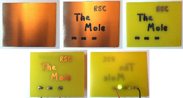
The pcb track pattern is made by etching away the unwanted copper to leave the desired interconnections. Firstly an etch-resistant pattern - the resist - is drawn on to the copper. This can be painted on using a suitable marker pen or screen print techniques can be used. The pcb is then placed in an etch which will remove all the bare uncovered copper, leaving the covered copper (the tracks) untouched. The steps to making a pcb are shown in the photos and include:
1) Cut the pcb to the correct size and clean to remove all dirt and grease
2) Drawn on the resist artwork pattern, shown in blue (I wrote 'The Mole' and 'RSC' and draw in three pads / connections for a resistor, LED and battery)
3) Etch for 10 to 15 minutes
4) Remove from etch and wash
5) Remove resist with solvent to reveal the copper tracks (see forth photo)
6) Drill and fit components through the holes
7) Solder components leads to the copper tracks. With the pcb turned over you can see the simple LED circuit on the fibre side of the board.
Various chemicals can be used as an etch to remove the copper. Nitric acid and ammonium persulphate can be used but ferric III chloride is standard. The reaction of copper with FeCl3 is a two step redox reaction:
FeCl3 + Cu → FeCl2 + CuCl
FeCl3 + CuCl → FeCl2 + CuCl2
Warming and agitating the etch solution (using vibrations and air bubbles) can greatly speed-up the process and produce a cleaner finish. After etching, cleaning and drilling, the pcbs are often dipped in a stannous chloride (SnCl2 ) compound to deposit a thin film of tin on the copper tracks. This provides a surface that does not tarnish as quickly as the pure copper but is still easy to solder. In addition to the chemical etching methods, modern CNC micro-milling machines are also being used to create pcbs. Channels can be cut into the bare copper using a tiny cutting tool to create complex tracks and wiring circuitry.
...............................................
THE CREATIVE SCIENCE CENTRE
Dr Jonathan Hare, The University of Sussex
Brighton, East Sussex. BN1 9QJ.
home | diary | whats on | CSC summary | latest news